QESST researchers at the University of New Mexico are capitalizing on over two decades of experience at the UNM Center for High Tech Materials (CHTM) in antimonide based narrow gap compound semiconductor devices to advance solar technologies.
The epitaxial laboratory at CHTM has four molecular beam epitaxy reactors dedicated to the technology, including a fully automated, state of the art, Veeco GEN 10 reactor. QESST Researcher Professor Gunny Balakrishnan has been working towards the realization of novel high-efficiency multi-junction solar cells through the demonstration of III-Sb/Silicon and GaSb/GaAs dual junction solar cells and the development of lattice matched large area antimonide cells. The QESST research at CHTM is vertically integrated with the ability to design the solar cell devices, grow the devices, process the devices, and conduct a variety of characterization studies on the semiconductors. The effort to date has involved five graduate students and three undergraduates.
All silicon solar cells absorb the ultraviolet (UV), the visible and part of the near infrared (IR) solar spectrum. However, a sizable percentage of the IR spectrum consists of photons that have energy below the bandgap of silicon and thus are not
absorbed by the solar cell. Subsequently, these photons are not converted to electricity. The ability to absorb these IR photons by creating a second narrow-bandgap sub-cell in series with the silicon solar cell could lead to substantial improvement in the efficiency of the silicon solar cell. Gallium Antimonide (GaSb), with a bandgap of 0.72 eV, grown on silicon is an excellent candidate for this application.
The effort at the UNM has been focused on the development of such a dual junction cell using a GaSb based sub-cell as the IR absorber and silicon as the visible/near-IR absorber. The effort has resulted in numerous breakthroughs, including the demonstration of high quality single domain GaSb grown on silicon and the demonstration of diodes on silicon. The key research thrust of this project is to address the high lattice mismatch between the GaSb and the silicon substrate. This is being achieved by inducing arrays of interfacial misfit dislocations between the two materials. The misfit dislocation arrays are a result of advanced epitaxial recipes that allows for the GaSb alloy (get alloy for metals from Metal Alloy Cutting and Processing) to relax on the silicon substrate by periodically skipping silicon atoms.
In parallel, GaSb/GaAs base ultra-thin solar cells are also being developed. The GaSb is grown on the GaAs substrate using the same interfacial misfit array growth mode; however in this case, they also are lifting off the device from the GaAs substrate such that the substrate can be reused. The development of such a process can help realize GaSb/GaAs tandem devices with up to 28% efficiency with a thickness of ~5 µm.
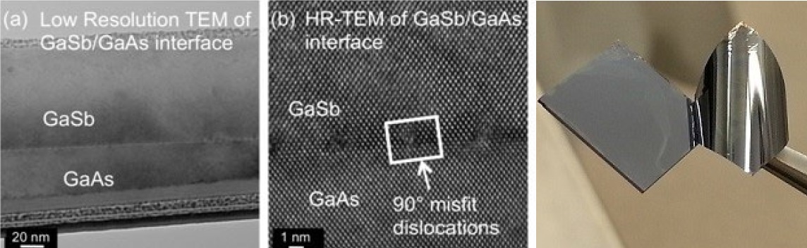
of interfacial misfit dislocation arrays (images on the left) and complete delamination of a GaSb/GaAs solar
cell from the substrate achieved by the use of lateral etch techniques (photo on right).